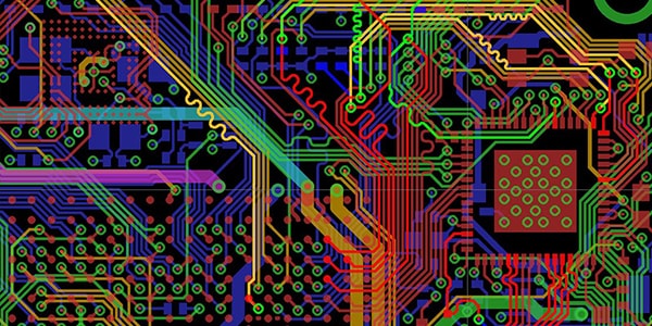
The working principle of PCB: the insulating material of the board base is separated by the conductive layer on the surface of the copper foil, so that the current can flow along the various components in the pre-designed circuit to complete the work, amplification, attenuation, modulation, demodulation, coding and so on. Next, a turnkey PCB assembly company will teach you how to design a PCB circuit.
Design of single-sided PCB board
The most basic circuit board is a single-sided board, with parts concentrated on one side and wires on the other. There must be proper electrical connections between the two layers of the PCB, the bridges between these circuits we call vias. Since the single panel is relatively simple, its design only requires the following four steps:
(1) Circuit schematic design: use ProtelDXP schematic editor to draw circuit schematic design.
(2) General professional PCB turnkey manufacturers will generate network reports. Its purpose is to show the connection between the circuit principle and the various components. Web reports are the bridge and link between circuit schematic design and circuit board design. FS Technology can quickly find the connection between components through the network report of the circuit principle table, thus providing convenience for the subsequent PCB design. .
(3) FS Technology refers to the design of printed circuit boards as PCB design. That is, converting the circuit schematic into its final form. This part of the design is more difficult than the design. We can use the powerful design of Protel. Function DXP to complete this part.
(4) After FS Technology completes the circuit board design, it will generate various reports, such as generating pin reports, circuit board information reports, network status reports, etc., and finally print out the printed circuit diagram.
Design Tips
Physical method: Manually cut off excess copper on the circuit board by using various cutting tools and power tools.
The methods most developers use today are chemical methods. In this way copper can be used unnecessarily when etching. The ability to cover the copper clad laminate with a protective layer is its greatest strength. During the production process, there are many ways to cover the protective layer. The most traditional methods include hand-painting and custom stickers. At present, the most used methods are the thin film photosensitive method and the thermal transfer PCB board method developed in recent years.
Photosensitive film printing PCB circuit board diagram
FS Technology will use a brush or hard pen to draw on the blank copper clad laminate, and after drying, it can be directly put into the caustic solution.
Various stickers and discs are available in the market. We need to paste it to the blank circuit board according to different organizations, as for the combination form, it is completely according to the user’s needs.
FS Technology will use photosensitive film to print the PCB circuit board diagram, and pre-coat a layer of photosensitive material on the blank copper clad laminate (there are copper clad laminates available on the market). After exposure, development, fixing and cleaning in a dark room environment, the solution will corrode the PCB circuit board, which must be paid attention to.
Thermal Transfer: Print the circuit directly onto a blank circuit board and then etch it with an etchant.
For the vast majority of electronic manufacturing companies, it is not cost-effective to make their own PCB boards. For this part of the company, we think that we can try FS Technology’s PCB manufacturing. Maybe you are not very familiar with FS Technology, we are the best one-stop PCB assembly manufacturer in China. From the moment you place an order on our website it starts working for you. Our services include Design-PCB Fabrication-Assembly-Test-Delivery. You can rest assured that we are the best turnkey PCB company in China.
Advantages and disadvantages of rapid PCB manufacturing:
FS Technology found the following disadvantages when using physical methods. This method is labor-intensive, time-consuming, difficult to control and irreversible. Because of these shortcomings, more and more PCB manufacturers will eliminate it and not use it. At present, when making PCB boards, we only use them when making simple circuits.
The process of chemical method is more complicated, but the precision is controllable, but there are still many uncontrollable factors. FS Technology uses this method the most when making PCBs.
Printing accuracy depends on the accuracy of the printer cartridges used.
The exposure and development time of the photosensitive plate is not easy to control. Because the optimal exposure time of each batch of printing plates will also be different, it takes repeated experiments to master.
When etching, the whole process is very difficult to control. We need to use professional control equipment to complete the large-scale production of the circuit board factory. When making PCBs, the temperature, concentration and pH value of the corrosion solution have a great influence on the corrosion quality.If you want to make a circuit board, you have to have a lot of experience. . Otherwise, material scrapping is serious.
We need to place the photosensitive plate in a dark room at low temperature. Of course, when exposing, you also need to keep the environment dark.
Summarize
To sum up, the traditional physical method of plate-making is labor-intensive, time-consuming and low-precision. Both physical and chemical methods require high skill, so neither method can be said to help engineers quickly achieve prototype PCB assembly production.

